International Journal of
Physical Sciences

  • Abbreviation: Int. J. Phys. Sci.
  • Language: English
  • ISSN: 1992-1950
  • DOI: 10.5897/IJPS
  • Start Year: 2006
  • Published Articles: 2572

Full Length Research Paper

Effect of annealing temperature on the optical properties of Sb-ZnO thin films prepared using co-sputtering technique

Hend Alkhammash
  • Hend Alkhammash
  • Department of Physics, Faculty of Sciences, Taif University, Taif 888, Saudi Arabia.
  • Google Scholar


  •  Received: 20 April 2018
  •  Accepted: 30 May 2018
  •  Published: 16 June 2018

 ABSTRACT

Transparent conducting oxide thin films of Sb-ZnO were prepared on optically flat quartz by radio-frequency (RF) sputtering method. The scan electron microscope was used to characterize the topological morphology of the surface of the as-prepared and annealed films at (300, 400, 470, and 525°C) for 4 h in air. The optical properties of the films were deliberated using their reflectance and transmittance spectra at normal incident light. The optical energy band gap energy (Eop ) values were found to increase by elevating the annealing temperatures. The dispersion curves of the refractive index of Sb-ZnOthin films were found to follow the single oscillator model. Optical parameters such as refractive index, real and imaginary parts of the dielectric constant, and optical conductivity were investigated.
 
Key word: Sputtering, thin film, Sb-ZnO, optical gap, refractive index.


 INTRODUCTION

Zinc oxide is an auspicious material for optoelectronic devices due to its big band gap (3.37 eV). The n-type zinc oxide materials can be acquired by doping with Aluminum, Gallium or Indium. Besides, p-type ZnO considered to be low resistivity and high mobility it is hard to be fabricated with good quality, where, it is related to the construction of native donor defects such as Oxygen vacancies and Zinc interstitials (Look et al., 1999). The most used acceptor dopants for p-type zinc oxide is antimony Sb, nitrogen, and phosphorous (Minegishi et al., 1997; Lu et al., 2004; Joseph et al., 1999; Chen et al., 2005; Limpijumnong et al., 2005; Zhao et al., 2003).  Doping ZnO with Sb was supposed to substitute Zn atom (Limpijumnong et al., (2004).  Xiu et al. (2005) have carried out p-type ZnO:Sb film by molecular beam epitaxy  and pulsed laser deposition (Xiu et al., 2005; Pan et al., 2007; Zi-Wen et al., 2010; Liang et al., 2015) confirming that Sb is a promising dopant for realizing p-type zinc oxide. Doping zinc oxide with tin oxide reveal that, increasing the content of tin oxide, ZnO nanocrystal changed from near spherical to dumbbell-like (Duan et al., 2017). Thermal annealing processing is used to enhance the properties of semiconductor material. Electro-deposition of Sb2S3 absorber on TiO2 nanorod array as photocatalyst for water oxidation has been investigated (Hong et al., 2018).  As far as the author 
 
know, the effects of thermal annealing on Sb-doped ZnO thin films are rarely reported. So, this work focused on the effect of thermal annealing on the optical properties of Sb-ZnO.


 EXPERIMENTAL TECHNIQUE

Thin films of Sb-ZnO were deposited on pre cleaned quartz substrates using sputtering unit model UNIVEX 350.The targets of ZnO and Sb are from Cathay Advanced Materials Limited Company. The base pressure of about 10–6 torr and sputtering pressure of about 2×10⁻² torr. The distance between the substrate and target was 10 cm with an angle 65°. The standers cubic centimeter per minute (sccm) was kept constant  at 20 cm3/min with rotation of substrate 2 rpm. The power on ZnO and Sb targets was kept constant of 100 W and 20 W respectively. The rate of deposition was kept at 2 nm/min. The thickness of the films were determined using multiple-beam Fizeau fringes in reflection (Tolansky, 1949). The scanning electron microscope (SEM) (Hitachi S4700) was used for characterizing the surfaces of the films. The double beam spectrophotometer (JASCO model V-670 UV–Vis–NIR) was used for detecting the transmittance T(λ) and reflectance at  R(λ) at nearly normal incidence in the range of wavelength 300 to 1800 nm. The absolute values of T(λ) and R(λ) are given by El-Nahass (1992).
 
 
where t is the film thickness.


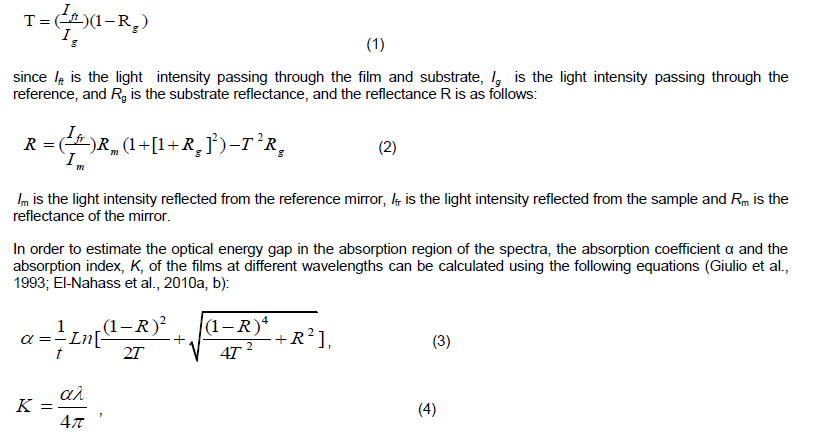
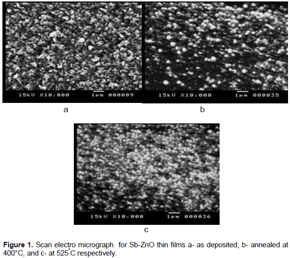
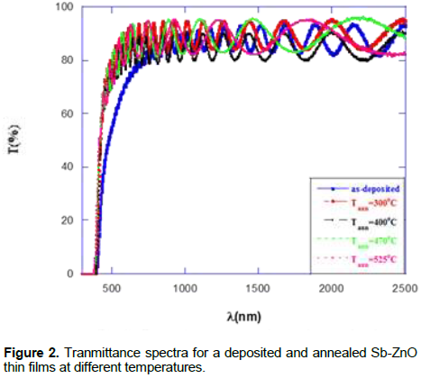
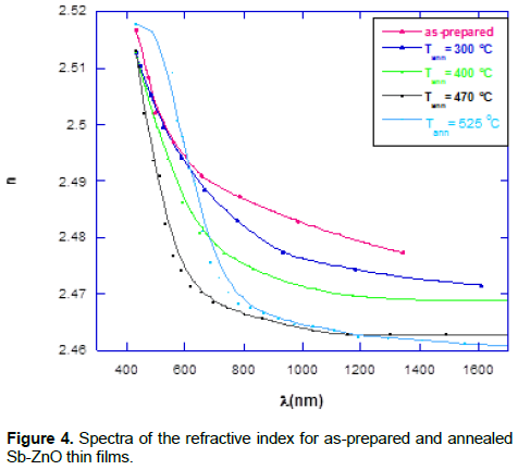
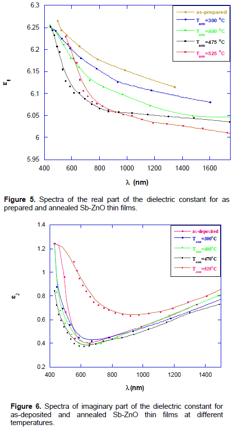
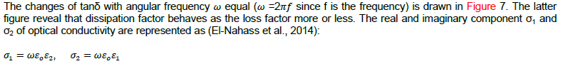
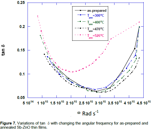
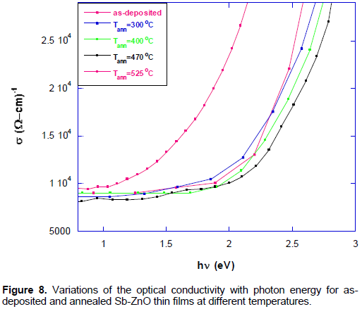
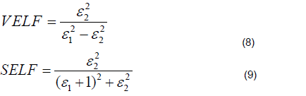
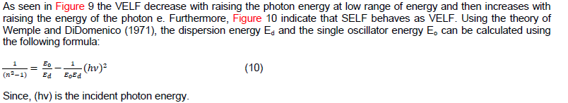
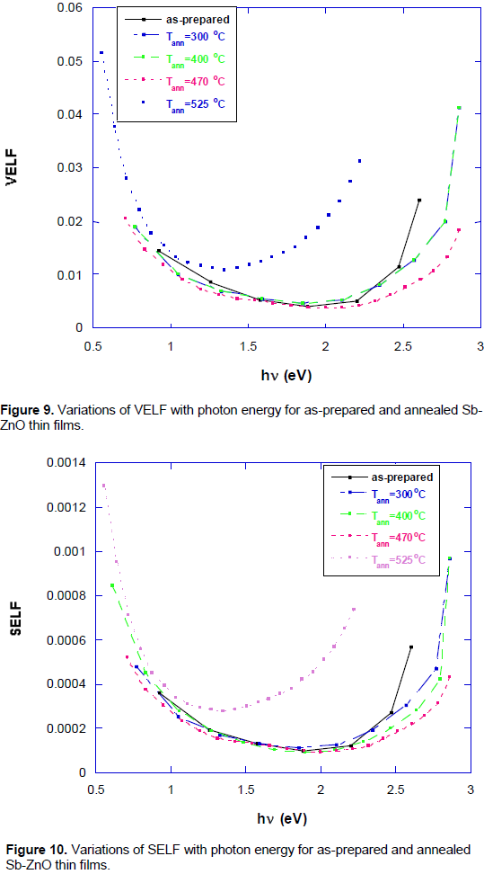
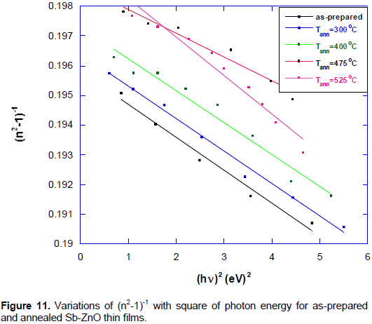
 RESULTS AND DISCUSSION

As shown in Figure 1a, the scan electron micrograph of the as-deposited film contain big grains besides, the films annealed at 400 and 525°C show more tighter crystal grains and the grain volume became smaller as shown in Figure 1b, c. This change in grain size is due to annealing which gaining the atoms of the thin films extra energy, and enhance crystallinity of the films; also, annealing can activate the Sb-as an acceptor (Zhao et al., 2011).
 
 
The transmittance spectra of Sb-ZnO thin films are shown in Figure 2 which reveal an excellent surface quality and homogeneity of the films due to the appearance of interference fringes (Abd El-Raheem et al., 2009). It is observed that, sharp interference fringes appeared and indicated that the air/layer and layer/glass interfaces are flat and parallel (El-Nahass et al., (2010b). Figure 2 shows also that the transmittance increased with elevating the annealing temperature, this is attributed to the decrease of the size of the particle.
 
 
The optical energy Eop was depicted from Figure 3 representing the plots of versus (hν) revealing that the direct optical gap widened with elevating the annealing temperature, this may be due to atomic rearrangement during the annealing process. Therefore, some defects will be removed leading to minimizing the density of dangling bonds causing the widening of optical gap (Mansour et al., 2010).  Another interpretation of this widening may be due to an enhancement in the crystalline structure of the film, since, if the film becomes more polycrystalline, a decrease in the band gap defects leading to band gap band gap broadening (Atta et al., 2016). Using Swanepoel, (1983, 1984) and Manifacier et al. (1976) methods, the refractive index of refraction n can be calculated. The index of refractive n of the thin films can be calculated using the equations:


Figure 4 displays the refractive index spectra for the Sb-ZnO films suggesting normal dispersion behavior. Furthermore, n decreases with raising the annealing temperature according to increasing the transparency of the films with increasing annealing temperature (Mohamed et al., 2006), which is affirmed by our results. 
 
 
The dielectric function ε is characterized as , the real part ε1 = n2 – k2, the imaginary part ε2 = 2nk is of the dielectric constant representing the dispersion and absorption respectively. tanδ represents the loss

factor. The dispersion and absorption spectra for antimony doped zinc oxide thin films prepared under different annealing temperatures are inspected in Figures 5 and 6 respectively. It is evident that ε1 behaves as the n as seen in Figure 5 ε2 fundamentally shows a decrease with wavelength and then increase with prolongating the wave length depending on the annealing temperature as displayed in Figure 6 which is linked to the variation of absorption α with photon wavelength.


where  the permittivity of frees pace is εo . The spectra of σ1 are shown in Figure 8. It can be seen that σ1 increases by increasing photon energy as shown in Figure 8 which can be owed to the excitation of the electrons by photon energy (Shaaban et al., 2006).
 
 
The surface and volume energy loss functions (SELF and VELF) can be calculated by using the relations (El-Nahass et al., 2014):


The dispersion and the single oscillator energies are obtained from the slope and intercept of  the plot (n2 – 1)–1 versus (hν)2 as seen in Figure 11 for the Sb-ZnO thin films. The values of Ed and Eo are 30.5, 68.4, 68.5, 70.9, 62.3 eV, and 29.3, 13.4, 13.6, 14.1, 12.4 eV for the as-prepared and annealed film at 300, 400, 475, and 525°C respectively. It is obvious that the dispersion has a tendency to increase with raising the annealing temperature, whereas the single oscillator energy has a tendency to lower with elevating the annealing temperature.


 CONCLUSION

For preparing antimony doped zinc oxide thin films, the Co-sputtering technique was used. It was found that the optical gap increases with raising the annealing temperature. Normal dispersion describes the behavior of the refractive index, and optical conductivity increase with raising the incident photon energy. Dispersion energy has a tendency to increase with raising the annealing temperature, whereas single oscillator energy has a tendency to lower with raising annealing temperature. Surface and volume energy loss functions found to depend on photon energy.


 CONFLICT OF INTERESTS

The author has not declared any conflict of interests.


 REFERENCES

Abd El-Raheem MM, Ali HM, El-husainy NM (2009). Characterization of electron beam evaporated CdTe thin films for optoelectronic devices. Journal of Optoelectronics and Advanced Materials 11(6):813-819.


Atta AA, El-Nahhas MM, Elsabawy M, AbdEl-Raheem MM, Hasaanien AM, Alhuthali A, Merazga A (2016). Optical characteristics of transparent samarium oxide thin films deposited by the radio-frequency sputtering technique. Pramana 87(5):72.
Crossref


Chen LL, Lu JG, Ye ZZ, Lin YM, Zhao BH, Ye YM, Zhu LP (2005). p -type behavior in In–N codoped ZnO thin films. Applied Physics Letters 87(25):252106.
Crossref


Duan M, Wang J, Liu C, Xie J, Han J (2017). Effects of SnO doping on the optical properties of ZnO in glass. Journal of Non-Crystalline Solids 459:32-35.
Crossref


El-Nahass MM (1992). Optical properties of tin diselenide films. Journal of Materials Science 27(24):6597–6604.
Crossref


El-Nahass MM, Atta AA, Abd El-Raheem MM, Hassanien AM (2014). Structural and optical properties of DC Sputtered Cd2SnO4 nanocrystalline films. Journal of Alloys and Compounds 585:1-6.
Crossref


El-Nahass MM, El-Deeb AF, Metwally HS, El-Sayed HEA, Hassanien AM (2010b). Influence of X-ray irradiation on the optical properties of iron (III) chloride tetraphenylporphyrin thin films. Solid State Sciences 12(4):552-557.
Crossref


El-Nahass MM, El-Deeb AF, Metwally HS, Hassanien AM (2010a). Structural and optical properties of iron (III) chloride tetraphenylporphyrin thin films. The European Physical Journal Applied Physics 52(1):10403.
Crossref


Giulio M Di, Micocci G, Rella R, Siciliano P, Tepore A (1993). Optical Absorption of Tellurium Suboxide Thin Films. Physica Status Solidi (a) 136(2):K101–K104.
Crossref


Hong J-Y, Lin L-Y, Li X (2018). Electrodeposition of Sb2S3 light absorbers on TiO2 nanorod array as photocatalyst for water oxidation. Thin Solid Films 651:124-130.
Crossref


Joseph M, Tabata H, Kawai T (1999). p-Type Electrical Conduction in ZnO Thin Films by Ga and N Codoping. Japanese Journal of Applied Physics 38(Part 2,11A):L1205–L1207.


Liang H, Chen Y, Xia X, Feng Q, Liu Y, Shen R, Du G (2015). Influence of Sb valency on the conductivity type of Sb-doped ZnO. Thin Solid Films 589:199-202.
Crossref


Limpijumnong S, Li X, Wei SH, Zhang SB (2005). Substitutional diatomic molecules NO, NC, CO, N2, and O2: Their vibrational frequencies and effects on p doping of ZnO. Applied Physics Letters 86(21):211910.
Crossref


Limpijumnong S, Zhang SB, Wei SH, Park CH (2004). Doping by Large-Size-Mismatched Impurities: The Microscopic Origin of Arsenic- or Antimony-Doped p -Type Zinc Oxide. Physical Review Letters 92(15):155504.
Crossref


Look DC, Hemsky JW, Sizelove JR (1999). Residual Native Shallow Donor in ZnO. Physical Review Letters, 82(12):2552-2555.
Crossref


Lu J G, Ye ZZ, Zhuge F, Zeng YJ, Zhao BH, Zhu LP (2004). p-type conduction in N–Al co-doped ZnO thin films. Applied Physics Letters, 85(15):3134-3135.
Crossref


Manifacier JC, Gasiot J, Fillard JP (1976). A simple method for the determination of the optical constants n, k and the thickness of a weakly absorbing thin film. Journal of Physics E: Scientific Instruments 9(11):1002-1004.
Crossref


Mansour B, Shaban H, Gad S, El-Gendy Y, Salem MA (2010). Effect of Film Thickness, Annealing and Substrate Temperature on the Optical and Electrical Properties of CuGa0.25In0.75Se2 Amorphous Thin Films. Journal of Ovonic Research 6(1):13-22


Minegishi K, Koiwai Y, Kikuchi Y, Yano K, Kasuga M, Shimizu A (1997). Growth of p-type Zinc Oxide Films by Chemical Vapor Deposition. Japanese Journal of Applied Physics 36(Part 2, 11A):L1453–L1455.


Mohamed HA, Ali HM, Mohamed SH, Abd El-Raheem MM (2006). Transparent conducting ZnO-CdO thin films deposited by e-beam evaporation technique. The European Physical Journal Applied Physics, 34(1):7-12.
Crossref


Pan X, Ye Z, Li J, Gu X, Zeng Y, He H, Zhu L, Che Y (2007). Fabrication of Sb-doped p-type ZnO thin films by pulsed laser deposition. Applied Surface Science, 253(11):5067-5069.
Crossref


Shaaban ER, El-Kabnay N, Abou-sehly AM, Afify N (2006). Determination of the optical constants of thermally evaporated amorphous As40S60, As35S65 and As30S70 using transmission measurements. Physica B: Condensed Matter, 381(1-2):24-29.
Crossref


Swanepoel R (1983). Determination of the thickness and optical constants of amorphous silicon. Journal of Physics E: Scientific Instruments 16(12):1214-1222.
Crossref


Swanepoel R (1984). Determination of surface roughness and optical constants of inhomogeneous amorphous silicon films. Journal of Physics E: Scientific Instruments 17(10):896-903.
Crossref


Tolansky S (1949). Multiple-Beam Interferometry Surface and Films, London: Oxford University Press.


Wemple SH, DiDomenico M (1971). Behavior of the Electronic Dielectric Constant in Covalent and Ionic Materials. Physical Review B 3(4):1338-1351.
Crossref


Xiu FX, Yang Z, Mandalapu LJ, Zhao DT, Liu JL, Beyermann WP (2005). High-mobility Sb-doped p-type ZnO by molecular-beam epitaxy. Applied Physics Letters 87(15):152101.
Crossref


Zhao B, Yang H, Du G, Miao G, Zhang Y, Gao Z, Fang X (2003). High-quality ZnO/GaN/Al2O3 heteroepitaxial structure grown by LP–MOCVD. Journal of Crystal Growth, 258(1-2):130-134.
Crossref


Zhao Z, Hu L, Zhang H, Sun J, Bian J, Zhao J (2011). Effect of different annealing temperature on Sb-doped ZnO thin films prepared by pulsed laser deposition on sapphire substrates. Applied Surface Science 257(11):5121-5124.
Crossref


Zi-Wen Z, Li-Zhong H, He-Qiu Z, Jing-Chang S, Ji-Ming B, Kai-Tong S, Xi C, Jian-Ze Z, Xue L, Jin-Xia Z (2010). Effect of Different Substrate Temperature on Sb-Doped ZnO Thin Films Prepared by Pulsed Laser Deposition on Sapphire Substrates. Chinese Physics Letters 27(1):017301.
Crossref


          */?>