ABSTRACT
Zinc sulphide (ZnS) thin films have been prepared by chemical bath deposition method. X-ray diffraction (XRD) is used to analyze the structure and crystallite size and scanning electron microscopy is used to study the particle size and morphology of ZnS thin film. Optical studies have been carried out using UV-Visible-NIR absorbance spectrum. The band gap value of the film is calculated and it is found to be 3.45 eV. The dielectric properties of ZnS thin films have been studied in the different frequency at different temperatures.
Key words: Zinc sulphide (ZnS) thin films, X-ray diffraction (XRD), scanning electron microscopy (SEM), dielectric studies.
Zinc Sulphide (ZnS) belongs to II-VI group compound with wide direct band gap value ranging from 3.4 to 3.70 eV. Zinc sulfide has cubic or hexagonal crystal structure or both at the same time. ZnS has significant potential applications such as in antireflection coating for light emitting diode (Katayama et al., 1975) for heterojunction solar cells (Bloss et al., 1988) and other optoelectronic devices such as electro luminescence devices and photovoltaic cells which are used in the field of displays (Beard et al., 2002), blue light emitting diode (Coe et al., 2002) sensors and lasers (Klimov et al., 2000) etc. In recent years nanocrystalline ZnS attracts much consideration because the properties in nano form vary significantly from those of their bulk.
Therefore, effort has been made to control the size, morphology and crystallinity of ZnS thin film in a wide variety of applications (Mach and Mueller, 1991; Varitimos and Tustison, 1987). ZnS thin films have been prepared by various methods such as thermal evaporation (Dimitrova, 2000), spray pyrolysis (Mustafa et al., 2007), sputtering (Shao et al., 2003), chemical vapor deposition (Icimura et al., 1999), successive ionic layer adsorption and reaction (Nomura et al., 1995), and metal organic vapour phase epitaxy (MOVPE) (Roy et al., 2006). In the present investigation, we report the synthesis and characterization of ZnS thin films. The ZnS thin films were characterized by X-ray diffraction, and scanning electron microscopy (SEM), for microstructure and morphology respectively, while UV-VIS-NIR analysis and dielectric for optical studies.
The preparation of ZnS thin films is based on the chemical bath deposition method which was carried out by dissolving zinc acetate and thiourea in double distilled water and at the deposition temperature of 60°C. Then, ammonia solution was added slowly with constant stirring to form the complex and pH of 10 was achieved. The deposition was done by keeping the substrates vertically inside the chemical bath. Deposition time of five minutes was recorded and the films were rinsed in double distilled water and then dried in air atmosphere. The X-ray diffraction (XRD) pattern of the ZnS thin films was recorded by using a powder X-ray diffractometer (Schimadzu model: XRD 6000 using CuKα (λ=0.154 nm) radiation, with a diffraction angle between 20 and 60°. The crystallite size was determined from the broadenings of corresponding X-ray spectral peaks by using Debye Scherrer’s formula. Scanning electron microscopy (SEM) studies were carried out on JEOL, JSM- 67001. The optical absorption spectrum of the ZnS thin films has been taken by using the VARIAN CARY MODEL 5000 spectrophotometer in the wavelength range of 300 to 600 nm. The dielectric properties of the ZnS thin films were analyzed using a HIOKI 3532-50 LCR HITESTER over the frequency range 50Hz-5MHz.
X- ray diffraction analysis
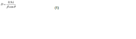
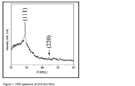
Structural identification of ZnS films has been done using with X-ray diffraction in the range of angle 2θ between 20° to 60° as shown in Figure 1. The excellent peaks (111) and (220) have been obtained. This film shows reflection along (111), (220) peaks corresponding to formation of hexagonal structure of ZnS. The broadened peak shows the nanometer-sized crystallites. The average nano-crystalline size (D) was calculated using the Debye-Scherrer formula:
where λ is the X-ray wavelength (CuKα radiation and equals to 0.154 nm), θ is the Bragg diffraction angle, and β is the FWHM of the XRD peak appearing at the diffraction angle θ. The average crystalline size is calculated from X-ray line broadening using (111) peak and Debye-Scherrer equation to be about 16.4 nm.
Scanning electron microscope (SEM)
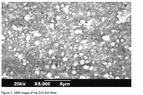
Scanning electron microscope (SEM) was used for the study of surface structure and roughness of the ZnS thin films. Figure 2 shows the SEM images of the ZnS thin films. The spherical crystallites which have the mean particle size of ~ 12 nm are visible through the SEM analysis.
UV-VIS-NIR spectral analysis
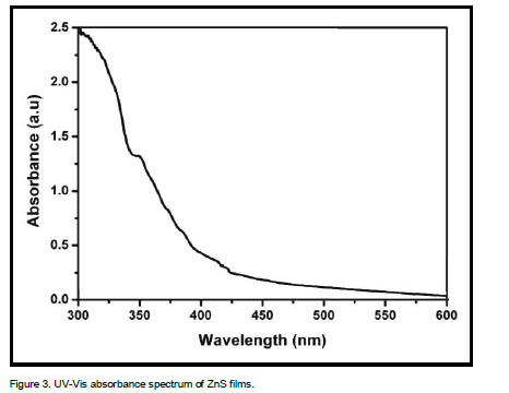
Study of materials by means of optical absorption provides a simple method for explaining some features concerning the band structure of materials. The optical absorption spectrum of ZnS films has been recorded in the wavelength region 300 – 600 nm and it is shown in Figure 3. It is important to note that ZnS films were highly transparent in the visible region. The absorption edge has been obtained at a shorter wavelength. The broadening of the absorption spectrum could be due to the quantum confinement of the ZnS thin films. As it is clear from spectrum, the films have a steep optical absorption feature, indicating good homogeneity in the shape and size of the nano-crystallines and low defect density near the band edge. Generally, the wavelength of the maximum exciton absorption decreases as the particle size decreases, as a result of the quantum confinement of the photo generated electron–hole pairs. The blue shift in the absorption spectrum is mainly attributed to the confinement of charge carriers in the nanoparticles. The dependence of optical absorption coefficient on photon energy helps to study the band structure and type of transition of electrons.
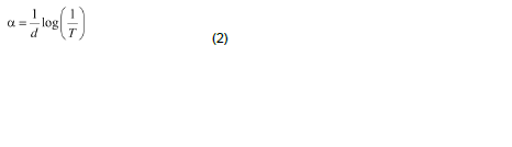
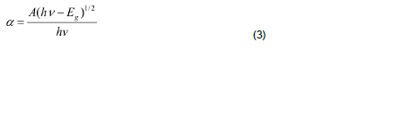
The optical absorption coefficient (α) was calculated from transmittance using the following relation:
where T is the transmittance and d is the thickness of the film. As a direct band gap material, the film under study has an absorption coefficient (α) obeying the following relation for high photon energies (hν):
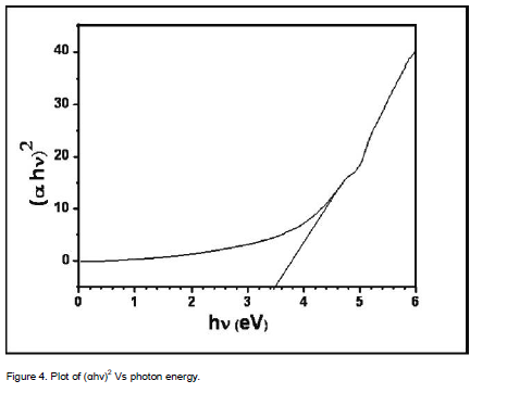
where Eg is the band gap of the ZnS films and A is a constant. A plot of variation of (αhν)2 versus hν is shown in Figure 4. Using Tauc’s plot, the energy gap (Eg) is found to be 3.50 eV which agrees well with the reported values (Shinde et al., 2011). The energy absorption gap is of direct type and the large band gap clearly indicates the wide transparency of the film. The result could be attributed to the quantum size effects as expected from the nanocrystalline nature of the ZnS thin films.
Dielectric properties
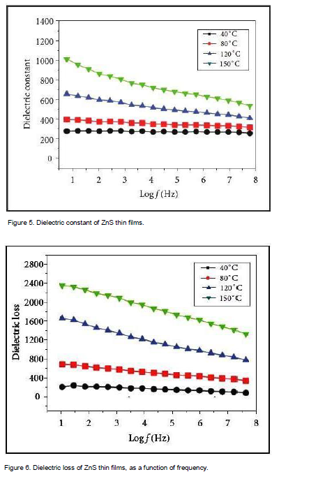
The dielectric properties of the ZnS thin films have been measured at different frequency and temperatures. The dielectric constant has been calculated with frequency at different temperatures as shown in Figure 5, whereas the following dielectric losses are depicted in Figure 6. Figure 5 showed that the dielectric constant decreases exponentially with increasing frequency and then reaches almost a constant value in the high frequency region. This also shows that the value of the dielectric constant increases with an increase in the temperatures. The large value of the dielectric constant is owing to the fact that ZnS thin films acts as a nanodipole under electric fields. The small-sized particles need a large number of particles per unit volume, ensuring increase of the dipole moment per unit volume, and a high dielectric constant (Suresh and Arunseshan, 2014). The decrease in the dielectric constant is due to electronic polarization which is quite less. Dipolar polarization is also expected to decrease with temperature as it is inversely proportional to temperature (Suresh, 2014). The polarizability of the space charge depends on the purity of the nanoparticles. As the temperature increases, the space charge effect towards polarization may have a tendency to increase (Sagadevan, and Sundaram, 2014). In Figure 6, the curves show that the dielectric loss is dependent on the frequency of the applied field, comparable to that of the dielectric constant. The dielectric loss decreases with an increase in the frequency at almost all temperatures, but appears to achieve saturation in the higher frequency range at all the temperatures (Sagadevan and Murugasen, 2014).
The Zinc sulphide (ZnS) thin films have been prepared by chemical bath deposition technique. Structural and morphology of the ZnS thin films were investigated by XRD and SEM. The XRD studies show the well crystallized and cubic structure of ZnS thin films. The UV-Visible absorbance spectrum shows excellent transmission in the entire visible region. The optical band gap is found to be 3.45 eV. The dielectric constant and dielectric loss of the ZnS thin films are calculated in the different frequency and temperatures.
The authors have not declared any conflict of interest.
REFERENCES
|
Beard MC, Turner GM, Schmuttenmaer CA (2002). Size-dependent photoconductivity in CdSe nanoparticles as measured by time-resolved tetrahertz spectroscopy. Nano Lett. 2:983. |
|
|
|
Bloss WH, Pfisterer F, Schock HW (1988). Advances in solar energy: An Annual review of research and development 4:275. |
|
|
|
Coe S, Woo WK, Bawendi MG, Bulovic V (2002). Electroluminescence from single monolayers of nanocrystals in molecular organic devices. Nature 420:800. |
|
|
|
Dimitrova JT (2000). Synthesis and characterization of some ZnS-based thin film phosphors for electroluminescent device applications. Thin Solid Films 365(1):134-138. |
|
|
Icimura M, Goto F, Ono Y, Arai E (1999). Deposition of CdS and ZnS from aqueous solutions by a new photochemical technique. 198-199, 308-312.
Crossref |
|
|
|
Katayama H, Oda S, Kukimoto H (1975). ZnS blueâ€lightâ€emitting diodes with an external quantum efficiency of 5×10⁻⁴. Appl. Phys. Lett. 27:657. |
|
|
|
Klimov VI, Mikhailovsky AA, Xu S, Malko A, Hollingsworth JA, Leatherdale CA, Eisler HJ, Bavendi MG (2002). Optical gain and stimulated emission in nanocrystal quantum dots. Science 290:314. |
|
|
|
Mach R, Mueller GO (1991). Physics and technology of thin film electroluminescent displays. Semicond. Sci. Technol. 6:305. |
|
|
|
Mustafa O, Bedir M, Ocak S, Yildirim RG (2007). The role of growth parameters on structural, morphology and optical properties of sprayed ZnS thin films. J. Mater. Sci. Mater. Electron. 18(5):505-512. |
|
|
|
Nomura R, Murai T, Toyosaki T, Matsuda H (1995). Single-source MOVPE growth of Zinc sulfide thin films using zinc dithiocarbarnate complexes. Thin Solid Films 271(1-2):4-7. |
|
|
|
Roy P, Ota JR, Srivastava SK (2006). Crystalline ZnS thin films by chemical bath deposition method and its characterization. Thin Solid Films 515(4):1912-1917. |
|
|
|
Sagadevan S, Murugasen P (2014). Structural and electrical properties of copper sulphide thin films by chemical bath deposition method. Int. J. Chem. Tech. Res. 6(14):5608-5611. |
|
|
|
Sagadevan S, Sundaram AS (2014). Dielectric properties of lead sulphide thin films for solar cell applications. Chalcogenide Lett. 11(3):159-165. |
|
|
Shao L, XChang KH, Hwang HL (2003). Zinc sulfide thin films deposited by RF reactive sputtering for photovoltaic applications. Appl. Surf. Sci. 212-213, 305-310.
Crossref |
|
|
|
Shinde MS, Ahirrao PB, Patil RS (2011). Structural, optical and electrical properties of nanocrystalline zns thin films deposited by novel chemical route. Arch. Appl. Sci. Res. 3(2):311-317. |
|
|
|
Suresh S (2014). Studies on the dielectric properties of CdS nanoparticles. Appl. Nanosci. 4:325-329. |
|
|
|
Suresh S, Arunseshan C (2014). Dielectric Properties of Cadmium Selenide (CdSe) Nanoparticles synthesized by solvothermal method. Appl. Nanosci. 4:179-184. |
|
|
|
Varitimos TE, Tustison RW (1987). Ion beam sputtering of ZnS thin films. Thin Solid Films 151:27. |